 |
 |
 |
 |
| back | |
|
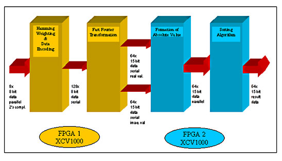
The following description shows how DSP functions - FFT and multiplications
- can be optimally designed to suit an FPGA by using its architecture
to advantage and by considering a number of possible design approaches.
|
|
|
|
|
|
One approach to the realisation of these functions using a combination
of FPGA and DSP chips was rejected, since the required performance
would have necessitated too many DSPs working in parallel. The functionality
of the FPGAs was described using the hardware description language
VHDL and by putting the Xilinx Core Generator to good use. Synthesis
was carried out using a generic tool. The Xilinx Floorplanner was
indispensable for the backend flow, allowing component placement
in a core with an impressive 98% LUT utilisation. VHDL It was clear from the outset that implementing this design on an
FPGA would demand a very high utilisation, so that resources would
have to be carefully allocated. On the other hand, the speed of
computation played a very important role, since the next set of
input data would be ready and waiting after 256ns. For this reason,
several approaches to the realisation were considered, and various
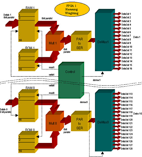
possibilities were tried out: For the second approach, the 8*8 bit multiplication was described with combinational logic (non-clocked), followed by the required number of register stages. The synthesis tool generated a clocked multiplication by assigning the register stages as appropriate within the multiplier. The main disadvantage with this approach is that the multiplier would have had to be replicated 128 times, which was just not possible with the resources available. The third approach also required the replication of a serial multiplier 128 times, which would have required a great many resources, if not quite as many as required by the second approach. The construction of a serial multiplier is described in more detail in the following FFT section. Implementing constant multipliers - the fourth approach - would of course have been ideal for realisation of the Hamming Weighting Window, however the 128 multipliers required in this case would have needed more than the available resources. Most suitable therefore, on account of the large number of simultaneous multiplication operations required, was the first approach. In all, only eight parallel multipliers were constructed, each
of which was used 16 times within each cycle. Since a new data set
is available every 256 ns, exactly 16 multiplications can be performed
using a system clock with 16ns period. The coefficients are stored
in eight ROMs, each 16 words deep. The ROMs are addressed using
the addresses for the RAMs in which the input data is stored. This
allows 128 parallel multiplications to take place within the allotted
256ns using only eight multipliers. Following the coefficient multiplication
stage, the data packets exiting each multiplier undergo parallel/serial
conversion and are subsequently divided into 16 serial data streams
for further processing in the following FFT stage. |
|
|
|
|
| FFT The Fourier Transform is used to determine the constituent frequencies of a time domain signal so that the signal can be described in the frequency domain, where it is easier to perform certain processing functions. The time domain signal is observed over a particular duration (sampling window) and sampled. The samples are used to calculate the frequency spectrum of the observed signal. A periodic signal with a frequency of f0 Hz would, under ideal conditions (well-chosen sampling window, no rounding errors), yield an amplitude maximum at frequency f0. The Fast Fourier Transform (FFT) allows optimisation of the computational effort by parallel processing of the input signal in the time domain. The 128-point FFT to be realised was built up in an entirely modular manner, in order to describe each module optimally with respect to data width and the required number of computations, and to reproduce each module only as often as necessary. As mentioned in the introduction, the FFT consists of seven stages (128 points = 27). The input data is eight bits wide - the result of the Hamming weighting - and increases by one bit at each stage to attain the precision required for this application. |
|
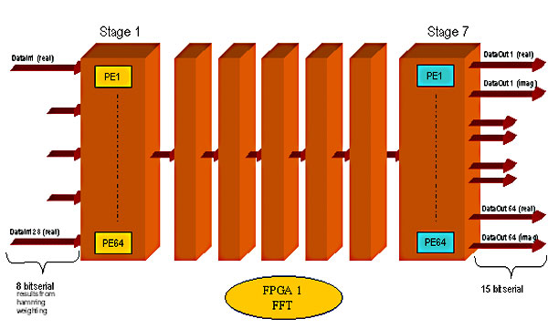 FFT consisting of seven Processing Stages |
|
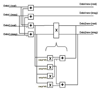
Each stage is in turn divided into the required 64 Butterfly processor elements. "Butterfly" refers to the characteristic construction of the processor element. Two data streams are input to the Butterfly, where, in its most elaborate form, the inputs represent complex numbers. These data streams consist of sine and cosine elements. The output of the Butterfly comprises two (usually complex) data streams. The computations within a Butterfly can be reduced to four real multiplications and six real additions, or three real multiplications and seven real additions, depending on which calculation can best be simplified. |
|
|
|
|
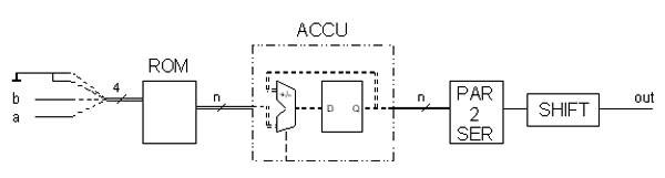
For 128 input data streams, 64 Butterfly PEs per FFT stage have to be constructed. The data remains in two's complement form all through the FFT. To keep the entire structure as simple as possible, it is necessary to consider which reductions can be carried out within each PE. For example, no complex data is present at the first stage, i.e. the imaginary elements in the PE can be ignored. Furthermore, the results of the multiplication with sine and cosine values of certain angles are easy to compute and do not require an entire Butterfly PE construction. For the construction of a complex PE, several possible approaches were tried as for the Hamming Weighting already described. For realising the multiplications, essentially the same approaches as in the previous chapter were considered. The possibilities for realising the additions were easy to determine - either serial or parallel, depending on the type of the preceding multiplications. Only the serial multipliers proved to be able to deliver the desired result, since all other approaches would have led to more than 100% utilisation of the FPGA. After all, several hundred multiplications are required, with increasing width. A serial multiplication with two's complement numbers is constructed as follows: For each calculation, two multiplications and the subsequent addition or subtraction are combined (see Fig.). The following two signed terms arise Acos(x) - Bsin(y) and Acos(x) + Bsin(y) Where x and y are constant for each Butterfly PE, and A and B represent the numbers to be multiplied. Under closer examination of the first term, we can see that, if A and B can only take on values of 0 or 1, there are only four possible results: 0, -sin(y), cos(x) and cos(x) -sin(y). These values are stored in ROMs and addressed using the address resulting from combining the data streams A and B. The ROM outputs then have to be accumulated together, since the ROM table has to be addressed a total of eight times for an 8-bit serial multiplication. The configurable accumulator of the Xilinx Core Generator is used to this end. Note that due to the two's complement representation of the values, the most significant bit must be subtracted and not added. Furthermore, care must be taken to erase the ROM contents at the address after each accumulation iteration, since these would present erroneous initial values for the next iteration. The results at the outputs are now ready, albeit in parallel form,
and must therefore undergo another parallel-serial conversion. Furthermore,
the timing must be adapted to the duration of the processing cycle.
Since new data arrives every 256ns, it makes sense to maintain this
time-frame throughout all stages. This is achieved by using area-efficient
SRLs (Shift Register LUTs). SRLs are by no means new components,
they simply feature an alternative switching within the LUT of the
CLB. In addition to other more complex functions, they can incorporate
a shift register of up to 16 bits in length, and are therefore very
economical as regards area. The shift registers become shorter and
shorter with each stage of the FFT, since the relevant data of the
serial data stream increases by one bit at each FFT stage, so that
the throughput through the functional part takes longer. Since the
last stage is 15 bits wide however, there is still enough time for
the necessary calculations.
|
|
|
|
|
| Absolute
Value
The absolute value of a complex number is usually calculated by squaring the real and imaginary parts, summing these and then calculating the square root of the sum. Since the absolute values in this case are only needed for a sorting operation, we can dispense with the square root. However, squaring means that two 15-bit values must be multiplied together, and this a total of 64 times. This gives in all 128 15-bit by 15-bit multiplications and 64 31-bit additions. None of the various possibilities considered yielded a solution that would have had room in the FPGA whilst satisfying the timing requirements. This method of calculating the absolute value could therefore not be implemented. An approximation formula was used instead, which fortunately does not adversely affect the result from a system point of view. To obtain the approximate value, the imaginary part is compared to the real part, and half of the smaller value is added to the larger value. Greatest errors arise only when both imaginary and real parts are equal. For practical purposes, the serial data from the FFT must first undergo a serial-parallel conversion. Then the presence of negative values must be determined. Should this be the case, a two's complement conversion is performed, since only the positive values are relevant for calculating the absolute value of the complex number. Two's complement conversion involves inverting all the bits and then adding a 1. This is achieved by EXOR-ing in a loop all the bits with the sign bit. If the sign bit is 0, the original bit values remain unchanged, if the sign bit is 1, the original bits are inverted. All that remains is to add the sign bit to the result to give the smallest possible realisation in hardware of a two's complement conversion. Comparing the two positive values, halving the lesser value by
a bit-shift to the right, and adding the two values are all described
in VHDL in such a way that the synthesis tool recognises what is
happening and utilizes the appropriate soft macros accordingly.
Sort The Sorter has to sort the absolute values according to size. The
biggest challenge here was to sort the 15-bit values within the
available 256ns, ready in time for the next set.
Conversion to Gates The interface between the first and second Virtex chip is located between the FFT and absolute value calculation. At this point, the data are presented in serial form, thereby satisfying the I/O capacities. Since the design is particularly Core-intensive, the synthesis, which regards the Cores as black boxes, was able to run through quite rapidly. However, it turned out that an automatic place-and-route was not possible with these chips. The first chip (performing Hamming Weighting and FFT) is utilized to 98%, whereby a great advantage is that the data flow is very straightforward. The data flow in the second chip is also quite straightforward while calculating the absolute values, but becomes more complicated when we reach the Sorter, since a large value located by the comparison tree has a direct influence on all the preceding stages of the tree. Further difficulties in placing the components in this FPGA, and particularly when routing, is the fact that the second FPGA has several other functions as well as all of the block RAMs and a multitude of nets with high fanouts from the centre of the chip to the edges, which is where the block RAMs are located. This problem was addressed by replicating the functions driving these nets. The entire structure for both chips had to be created by manual
placement, which turned out to be very demanding. It was even necessary
to change the predefined placement macros for certain Core elements,
in order to be able to place them closer to other elements. The
Xilinx back end tools processed the design quite rapidly with the
aid of the generated floorplan files, and yielded the desired result
which was then verified by static timing analysis and appropriate
timing simulations.
Conclusion To conclude this - at times very detailed description - it is worth noting that, for this application, the effort in trying out various approaches using small examples with an eye towards timing and the available resources certainly paid off, since without this structured and detailed preparatory work, the entire project would have capitulated due to the complexity of the functions. The design was optimally adapted to suit the technology, for which detailed knowledge was required. This knowledge, combined a good measure of stamina and a willingness to try new approaches, made the realisation of the design possible. A different chip with a different technology would certainly have
demanded entirely different approaches to a solution. For example,
looking at the Xilinx VirtexII family - which could not be implemented
at the time - a realisation of this design would have been quite
different, and in some places would have been considerably easier
owing to the availability of the parallel multipliers. However,
these chips will also doubtlessly be faced with designs which take
them to their limits, demanding experience and an in-depth knowledge
of the tools and technology. |
|